2025 AIChE Annual Meeting
(189b) Tailored Separation Strategy for Highly Conductive Metallic Single-Walled Carbon Nanotubes Toward Electrode Applications
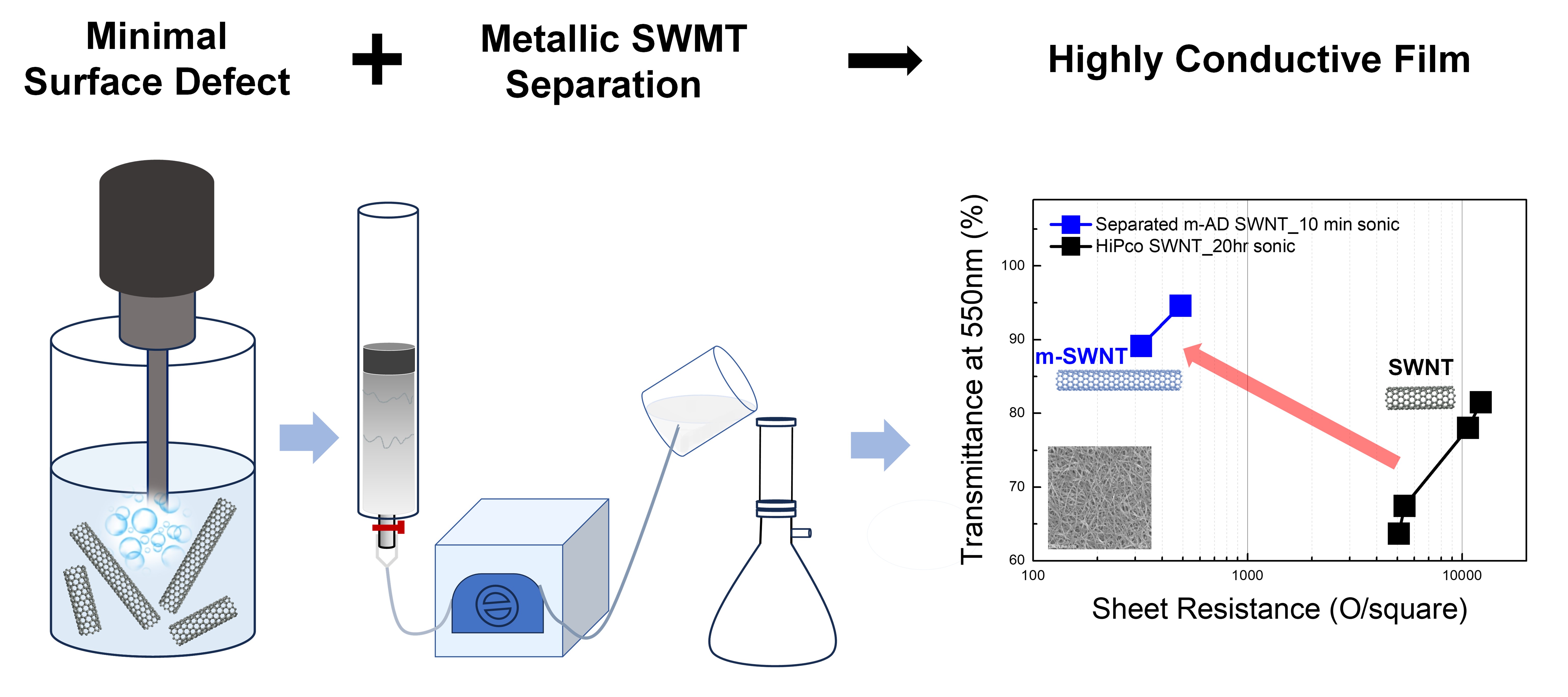
To address these limitations, this study proposes a dual optimization strategy: (i) controlling the ultrasonication dispersion conditions to minimize length-shortening and surface defects of the SWNTs, and (ii) employing high-efficiency gel chromatography to isolate high-purity m-SWNTs. The resulting SWNT films exhibit ultra-low sheet resistance, high transparency, and mechanical stability, showing great potential for next-generation batteries and optoelectronic devices.
Two commercially available SWNT types—HiPco and arc-discharge (AD) SWNTs—were compared in this study. AD SWNTs, with larger diameters (1.45–1.65 nm) and longer lengths (1–5 μm), showed better resistance to surface damage during ultrasonication compared to HiPco SWNTs (0.8–1.2 nm, 100–1000 nm). This is because AD SWNTs have structural characteristics that allow them to better endure the ultrasonication dispersion process. Each type was subjected to ultrasonication for 10 minutes, 2 hours, and 20 hours. Raman spectroscopy and atomic force microscopy (AFM) were used to investigate the increase in defects and reductions in length of SWNTs after sonication. The ID/IG values of the SWNT films increased with dispersion time, particularly for HiPco samples. According to AFM measurements, the length of AD SWNTs decreased from 1250 nm (10 min) to 125 nm (20 h), indicating the importance of balancing dispersion efficiency with structural preservation.
Electrode films fabricated from AD SWNT suspensions dispersed for 10 minutes exhibited excellent electrical performance, achieving a sheet resistance of 245 Ω/sq at a transmittance of 70%. When dispersion duration was increased to 2 hours, the sheet resistance moderately increased to 383 Ω/sq at 70% transparency, indicating slight defect generation on SWNT surface. A significant decline in electrical conductivity was observed after a prolonged dispersion of 20 hours, resulting in a dramatically higher sheet resistance of 1,940 Ω/sq at the same transmittance. In comparison, HiPco SWNT films showed consistently inferior performance than AD SWNTs under identical sonication conditions, with a sheet resistance of 400 Ω/sq after 10-minute dispersion, sharply increasing to 3,897 Ω/sq at 2 hours, and further deteriorating to 6,450 Ω/sq after 20 hours of ultrasonication. These results suggest that AD SWNTs have much higher resistance to surface damage over HiPco SWNT during sonication. These results also highlight the importance of optimizing dispersion conditions to balance structural preservation and electrical conductivity for high-performance SWNT electrode applications.
To further enhance conductivity, metallic SWNTs were separated from their original mixtures using gel column chromatography with Sephacryl S-200 gel. A mixture of sodium dodecyl sulfate (SDS) and sodium cholate (SC) at a 3:2 ratio was used as the surfactants. For the HiPco SWNTs, separation was conducted using a short column, and depending on the dispersion state, different multi-step separation strategies were applied. For samples dispersed for 20 hours and 2 hours, a six-layer separation approach was employed, whereas for the 10-minute dispersion, a three-layer separation was sufficient to separate metallic from semiconducting fractions. Metallic fractions were eluted through the column, while semiconducting fractions were trapped in the gel, leading to the separation of metallic from semiconducting fractions. Due to limitations in separation precision in a single pass, the collected metallic layers underwent re-separation to further purify and obtain clean, high-purity metallic SWNTs.
In contrast, AD SWNTs required a significantly different approach due to their structural properties. Separation was not successful in short columns and required long columns to facilitate proper separation of metallic from semiconducting SWNTs. That is, unlike HiPco SWNTs, semiconducting SWNTs are not effectively trapped in the gel and some semiconducting SWNTs are eluted together with metallic SWNTs, leading to the poor SWNT separation. Therefore, further fine-tuning of the column length, diameter, gel amount, and temperature to delay the elution of semiconducting species are necessary to obtain high-purity metallic SWNTs. Though AD SWNT separation demanded longer processing time due to flow rate adjustments, it allowed for precise separation of metallic and semiconducting SWNTs in a single run. Successful separation was confirmed by the disappearance of semiconducting SWNT absorption peaks in the UV-Vis-NIR spectrum in the separated metallic SWNTs.
The resulting m(metallic)-AD SWNT solutions from SWNT mixtures were confirmed to have high purity and structural stability by UV-Vis-NIR and Raman spectroscopy. Films fabricated from these solutions achieved sheet resistance of 335 Ω/sq at 90% transmittance. In contrast, films made from unseparated AD SWNTs showed 1616 Ω/sq under the same transmittance. Even films with 75.4% metallic purity exhibited limited improvements, indicating that >90% purity is essential for meaningful performance enhancement. Raman results also showed significantly reduced D-band intensity, indicating minimal structural damage after separation.
The effectiveness of the separation process was confirmed through recyclability tests. The Sephacryl gel maintained its separation efficiency over five reuse cycles, demonstrating its applicability to industrial production and environmental sustainability. This process reduces chemical and material waste and can be adapted to roll-to-roll production systems.
Analysis of the conductivity enhancement mechanism revealed that SWNTs with larger diameters and longer lengths reduced inter-tube contact resistance, enabling smoother charge transport. Lower D-band intensities correlated with fewer defects and better conductivity. These observations support percolation theory, which suggests that longer tubes form better conduction paths and less-defective tubes support more efficient electron transport. Additionally, the surfactant composition was key to preventing CNT bundling and improving film uniformity.
While previous research focused primarily on increasing m-SWNT content, often neglecting dispersion-induced damage, our approach simultaneously addresses purity and structural preservation. As a result, not only individual tube performance but also overall network conductivity was improved. The final SWNT films showed high flexibility and conductivity, making them suitable for electrode for various applications, i.e., lithium-ion battery, supercapacitors, and conductive film in electronic devices. Importantly, the method preserves the intrinsic properties of SWNTs without chemical doping or harsh surface modification.
This study presents a practical, scalable, and reproducible process for fabricating high-conductivity CNT-based electrodes. By combining dispersion control with optimized gel chromatography, we provide a flexible process platform for tailoring SWNT properties for various applications. Our study highlights that physical optimization—namely, maintaining tube length, minimizing structural defects, and isolating electronic type—is not only sufficient but essential to realizing the full potential of CNT-based electrodes. The results also deepen our understanding of structure–property relationships in carbon nanomaterials and how to control them through process engineering.
Future research will apply these m-SWNT films in actual battery cells to evaluate long-term cycling and electrochemical performance. Key considerations will include adhesion to current collectors, binder compatibility, and operational stability.
Beyond lithium-ion batteries, the transparent and conductive films fabricated through our method can serve in a wide range of optoelectronic and energy-harvesting applications. Potential target areas include transparent electrodes for organic solar cells, touchscreens, flexible displays, and electromagnetic interference (EMI) shielding layers. The films’ high optical transmittance (>90%), low sheet resistance, and mechanical flexibility make them particularly attractive for next-generation flexible and wearable electronics. Furthermore, the compatibility of our separation and dispersion process with various substrate types and solution-based fabrication methods suggests easy integration with current industrial processes.
Lastly, the insights gained in this work provide a blueprint for future exploration of structure–property–process relationships in nanomaterials. By coupling physical morphology control with post-synthesis electronic purification, the approach offers a new paradigm for engineering carbon-based materials at both the molecular and network levels. This foundation may extend to hybrid nanocomposites, multi-walled CNT systems, and 2D material heterostructures, thus opening new avenues in multifunctional energy storage, conversion, and sensing technologies.