2025 AIChE Annual Meeting
(189q) Enhancing Near-Infrared Detection in Organic Photodetectors with Planar Heterojunctions and Waveguide Patterning.
Typically, an OPD consists of an active layer containing an electron donor (D) and an electron acceptor (A) material. In a Planar Heterojunction (PHJ), these layers are stacked without polymer mixing. Upon light absorption, Frenkel excitons are formed. High-energy excitons recombine in the p-type layer, while lower-energy excitons diffuse to the donor-acceptor interface due to the energy difference between the p-type and n-type polymers. As a result, the PHJ structure strongly detects red and near-infrared (NIR) wavelengths.
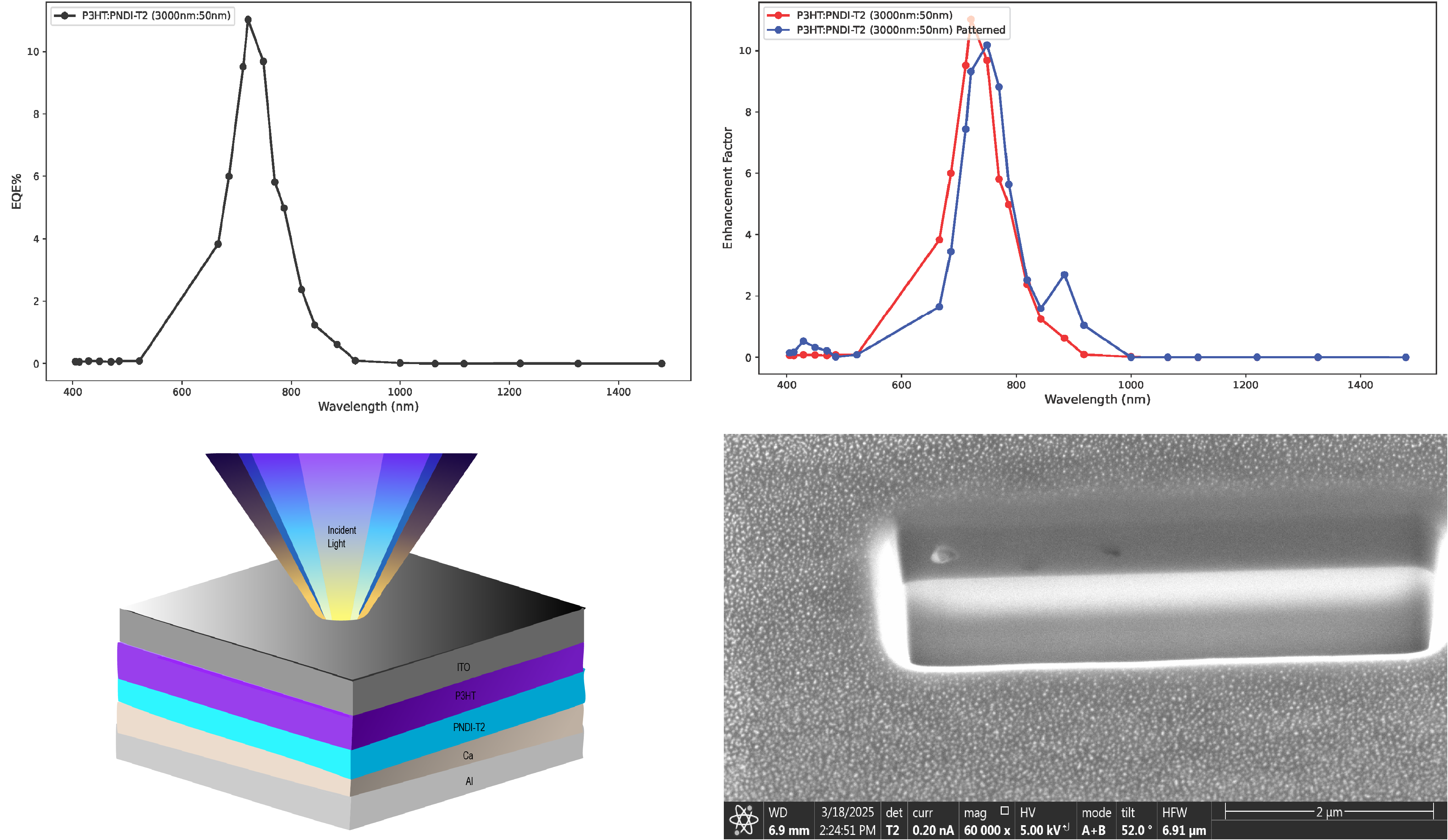
In our OPD devices, a thin layer of Poly{[N,N'-bis(2-octyldodecyl)naphthalene-1,4,5,8-bis(dicarboximide)-2,6-diyl]-alt-5,5'-(2,2'-bithiophene)} (PNDI-T2), an n-type polymer, is solution-deposited on top of a thick layer of poly(3-hexylthiophene-2,5-diyl) (P3HT), a p-type polymer, forming a planar heterojunction. This structure is achieved by doping the P3HT layer to make it insoluble, then coating PNDI-T2 on top, followed by dedoping the entire stack with 1-Butylamine. By adjusting the thickness of the optical cavity (P3HT and PNDI-T2 layers), we achieved a peak response at 721 nm, with a responsivity of 0.06 A/W, an external quantum efficiency (EQE) of 10%, and a full width at half maximum (FWHM) of 85 nm, without the need for optical filters, CIN, or CCN. The EQE can be tuned by varying the thickness of the p-type layer, enhancing the peak in the near-IR while suppressing ultraviolet and blue photons. So we demonstrate how to stack, pattern and create a unique photodetector using little chemical manipulation.
In addition to achieving narrowband absorption, we have patterned the p-type layer to create a waveguide structure at the D-A interface. This surface modification is a critical result, as it generates a cavity effect that significantly enhances the device's responsivity at longer wavelengths. As a result, we achieved a second detectivity peak at ~884 nm, with a detectivity of 0.012 A/W and an EQE of 2%. The process was successfully replicated with a different n-type polymer (WQ295), demonstrating the versatility of this technique and advancing the development of all-polymer devices.
Images:
Panel 1: Shows the external quantum efficiency of one of our photodetectors demonstrating it filters all light except the enhanced peak near 800nm.
Panel 2: Shows the external quantum efficiency of one of our photodetectors showing the same peak at at 800nm and in addition another smaller peak 900nm that comes from patterning a waveguide into it.
Panel 3: Schematic of Planar Heterojunction Organic Photodetector
Panel 4: Shows SEM image of the bilayer planar heterojunction, demonstrating there is no interface mixing.