2025 AIChE Annual Meeting
(17h) Electrochemical Cell Fabrication for Quasi 1-D Copper Electrodeposition
Authors
Kirk Ziegler, University of Florida
Farzam Zoueshtiagh, Universite de Lille
Ranga Narayanan, University of Florida
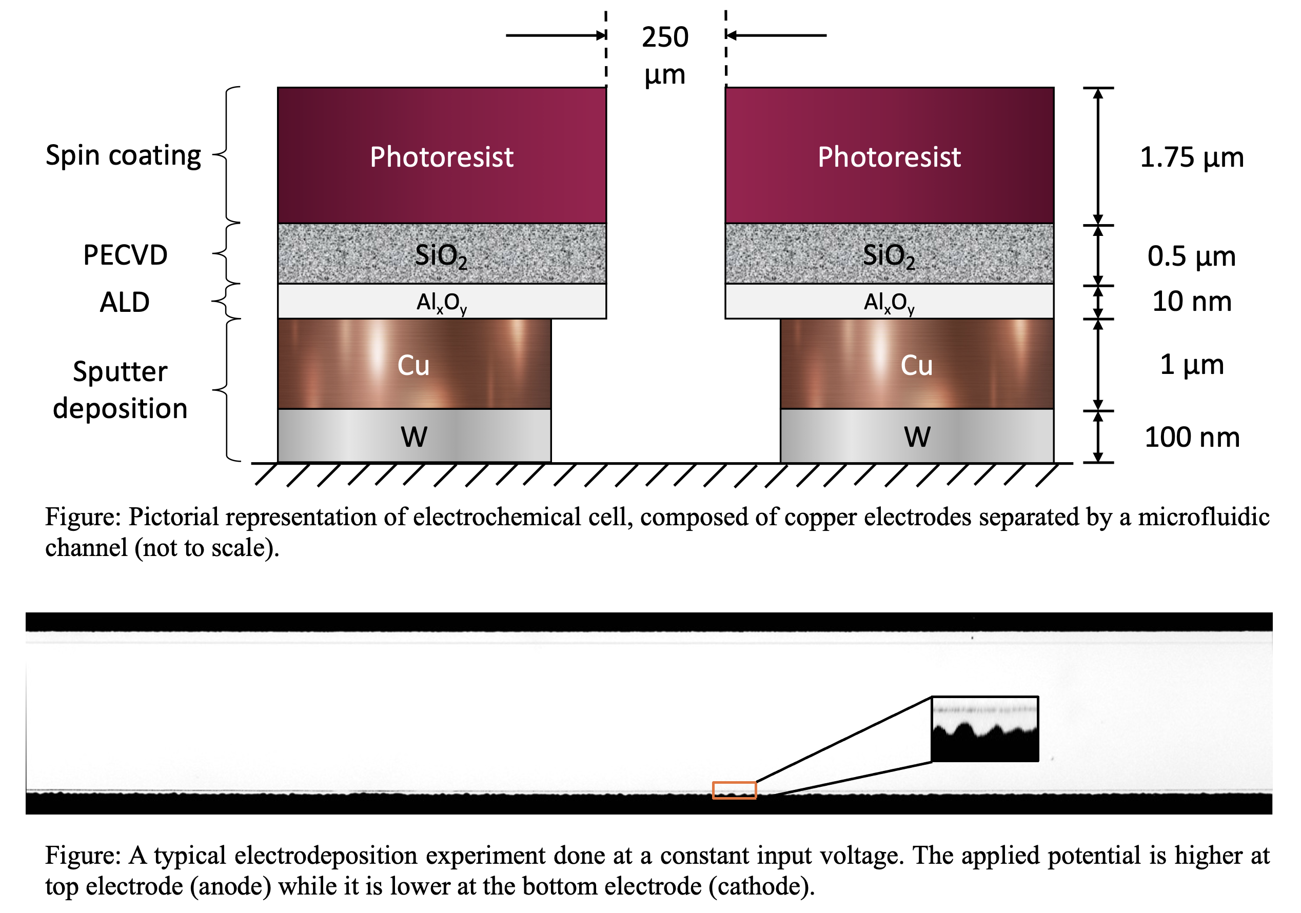
Controlled growth of copper dendrites has significant implications for next-generation electronics and energy storage applications. A key to studying these systems is designing electrochemical cells that control both transport and kinetics during electrodeposition. In this work, we demonstrate a modified methodology to fabricate electrochemical cells with an overhang that minimizes the corner effect on electrodeposition, allowing quasi one-dimensional growth of copper cells or dendrites when a small voltage is applied across the electrodes. The electrodes were fabricated on glass wafers through a multi-step process involving sputter deposition of metal layers, followed by dielectric layer growth via atomic layer deposition (ALD), and plasma-enhanced chemical vapor deposition (PECVD). The electrochemical cells were patterned on the wafer using photolithography and selective etching processes. The fabricated electrodes have been shown in the accompanying diagram. This process was investigated for two dielectric materials - silicon dioxide and silicon nitride. After etching to create the overhang, the compressive stresses in the dielectric film can lead to periodic buckling of the thin film with a characteristic wavelength, visible by the interference patterns under an optical microscope. These buckling phenomena cut off the contact between electrolyte solution and the metal electrode in specific regions, resulting in non-uniform electrodeposition patterns. Several strategies were explored to diminish the buckling phenomena of the dielectric film, including post-etching compressed air drying, slow oven drying, and critical point drying.