2024 AIChE Annual Meeting
(545f) From Powder to Large-Area Films - a Solution-Processable Route for Thin Films of Semiconducting 2D Tmds for Solar Energy Conversion
Authors
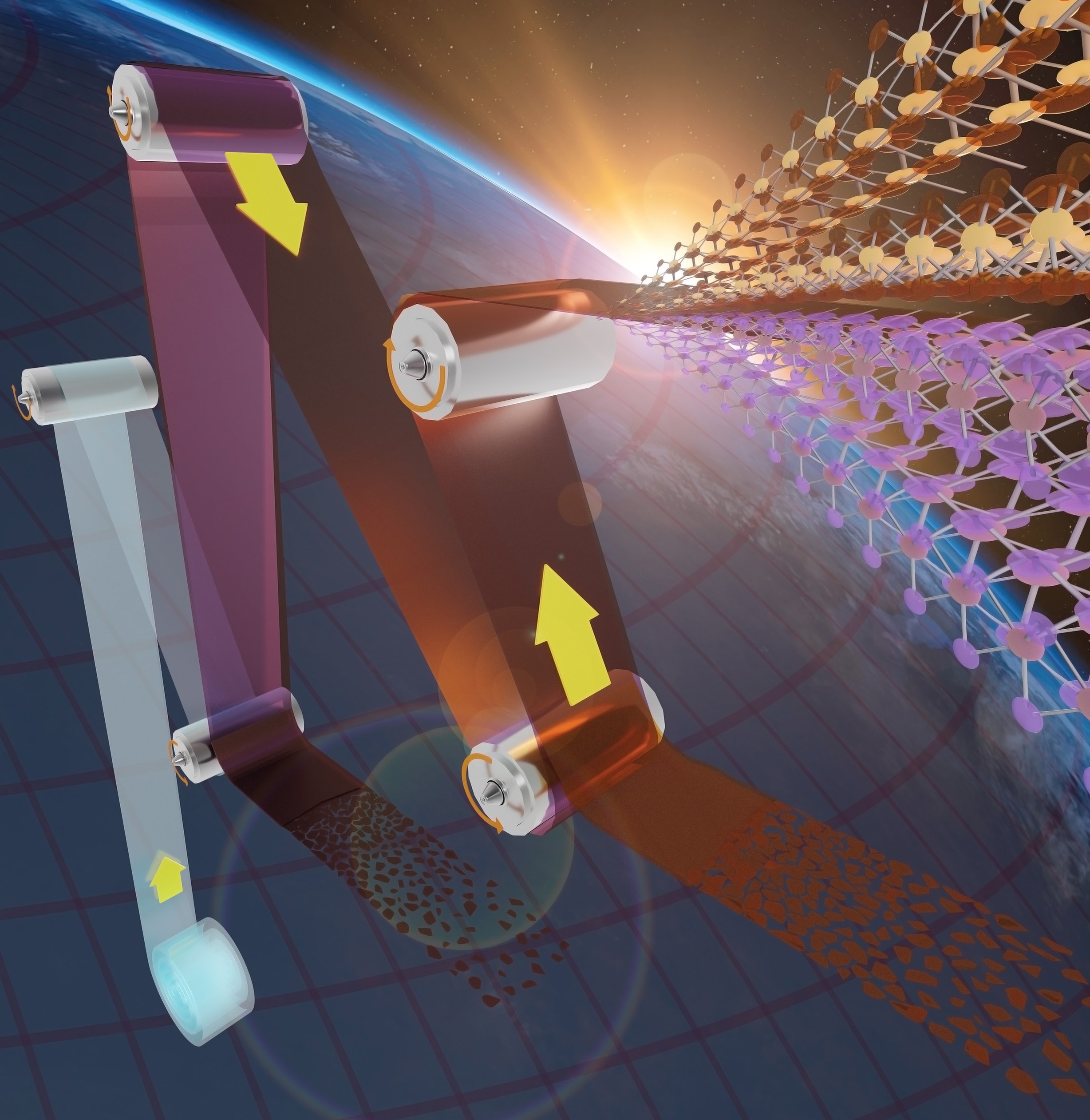
We address this issue by developing methods for the solution-based fabrication of nanoflake TMD thin films for incorporation in large area solar energy conversion devices2. In this presentation we highlight a novel method for exfoliating commercially available TMD powders via electrochemical pellet intercalation3. Compared to traditional solution-processable methods such as ultrasonication, this method results in nanosheets with superior optoelectronic and photoelectrochemical properties. These specially engineered nanoflakes show higher photocurrent densities (Jph), lower dark current densities (Jdark), and an absorbed photon-to-current efficiency (APCE) up to 90%. We examine the improved performance by comparing defect types and densities using fluorescent microscopy4 and atomic resolution scanning transmission electron microscopy (AR STEM) paired with an integrated differential phase contrast (iDPC) technique5.
To process our exfoliated materials into large-area thin films we report the further advancement of our preparation methods toward a continuous roll-to-roll deposition of TMD-based thin films from nanoflake dispersions using a liquid-liquid self-assembly technique6. We demonstrate reproducible printing of 100 mm wide TMD flake films on plastic substrates. Thus, we outline a pathway for fully solution-processable 2D-TMD devices beginning with as-received bulk TMD powder and finishing with large-area nano-flake thin films.
References
(1) Yu, X.; Sivula, K. Toward Large-Area Solar Energy Conversion with Semiconducting 2D Transition Metal Dichalcogenides. ACS Energy Lett. 2016, 1 (1), 315–322. https://doi.org/10.1021/acsenergylett.6b00114.
(2) Wells, R. A.; Sivula, K. Assembling a Photoactive 2D Puzzle: From Bulk Powder to Large-Area Films of Semiconducting Transition-Metal Dichalcogenide Nanosheets. Acc. Mater. Res. 2023, 4 (4), 348–358. https://doi.org/10.1021/accountsmr.2c00209.
(3) Wells, R. A.; Zhang, M.; Chen, T.-H.; Boureau, V.; Caretti, M.; Liu, Y.; Yum, J.-H.; Johnson, H.; Kinge, S.; Radenovic, A.; Sivula, K. High Performance Semiconducting Nanosheets via a Scalable Powder-Based Electrochemical Exfoliation Technique. ACS Nano 2022, 16 (4), 5719–5730. https://doi.org/10.1021/acsnano.1c10739.
(4) Zhang, M.; Lihter, M.; Chen, T.-H.; Macha, M.; Rayabharam, A.; Banjac, K.; Zhao, Y.; Wang, Z.; Zhang, J.; Comtet, J.; Aluru, N. R.; Lingenfelder, M.; Kis, A.; Radenovic, A. Super-Resolved Optical Mapping of Reactive Sulfur-Vacancies in Two-Dimensional Transition Metal Dichalcogenides. ACS Nano 2021, 15 (4), 7168–7178. https://doi.org/10.1021/acsnano.1c00373.
(5) Yücelen, E.; Lazić, I.; Bosch, E. G. T. Phase Contrast Scanning Transmission Electron Microscopy Imaging of Light and Heavy Atoms at the Limit of Contrast and Resolution. Sci Rep 2018, 8 (1), 2676. https://doi.org/10.1038/s41598-018-20377-2.
(6) Wells, R. A.; Johnson, H.; Lhermitte, C. R.; Kinge, S.; Sivula, K. Roll-to-Roll Deposition of Semiconducting 2D Nanoflake Films of Transition Metal Dichalcogenides for Optoelectronic Applications. ACS Appl. Nano Mater. 2019, 2 (12), 7705–7712. https://doi.org/10.1021/acsanm.9b01774.