2024 AIChE Annual Meeting
(4lb) Advanced Materials for Energy Efficient Devices: Taking 2D Materials from Lab to Fab.
Author
Research Interests
Performance improvements in integrated circuits (ICs) have been maintained through dimensional scaling. The miniaturization of the field-effect transistor (FET) followed the Dennard scaling but is reaching its limit due to doping complexity and gate leakage at extremely small length scales. Additionally, scaling rules necessitate channel thickness to be reduced with reduction in gate length to ensure sufficient electrostatics for suppressing short channel effects (SCEs). However, imperfections (dangling bonds) in bulk silicon result in a significant reduction in carrier mobility with channel thickness less than 4 nm. Atomically thin sheets of layered semiconducting materials like transition metal dichalcogenides (TMDCs) are promising for next generation electronic and optoelectronic devices due to their passivated surfaces which are free from dangling bonds. These atomically thin semiconductors have shown minimal scattering effects and high mobilities. Additionally, monolayers of these materials have unique properties making them ideal for applications in flexible electronics, spintronics, valleytronics, and optoelectronics. However, despite the enormous potential demonstrated by atomically thin sheets of these layered 2D materials, they are far from commercialization. Three major hurdles that have prevented the commercialization of 2D TMDCs are: (a) lack of scalable fabrication techniques for wafer scale synthesis of high quality TMDCs, (b) lack of doping techniques that avoid damage to ultrathin structures by energetic ions, and (c) issues related to high contact resistance.
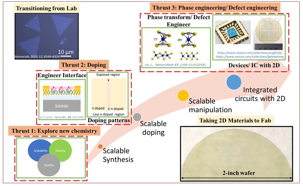
My research aims to address some of these hurdles preventing the translation of 2D materials from Lab to Fab are shown in Fig. 1. My unique research experience puts me in a position to assemble a group that can focus on addressing these issues facilitating the “Lab to Fab Translation” of 2D materials.
My research interests focus on the following thrust areas:
Thrust 1. Developing new chemistry for large area scalable growth of 2D materials.
Thrust 2. Doping these unique 2D materials at scale.
Thrust 3. Phase engineering TMDCs to address contact resistance issues.
Research Thrust 1: Using thermodynamics to drive new chemistry for wafer scale material synthesis.
Current approaches to wafer scale growth: chemical vapor deposition (CVD, with solid metal oxide precursors) and metal-organic CVD (MOCVD, with metal organic gaseous precursors) are the most common approaches for large area growth of 2D materials. While these approaches have led to successful wafer scale growth of monolayer 2D materials (including TMDCs), both approaches have several limitations.
- CVD is less controlled due to solid phase precursors oftentimes leading to inhomogeneity and lack of reproducibility. The defect density of samples grown by CVD is also quite high.
- MOCVD is better controlled due to gaseous precursors but oftentimes leads to carbon contamination due to the use of metal organic precursors. Additionally, MOCVD process is expensive and uses precursors which are toxic and difficult to handle.
Fig. 3a highlights comparisons of various vapor-based techniques currently used for 2D material growth. One can see that while CVD and MOCVD outperform the other techniques they are still far from the target for Lab to Fab Transition. Hence, new chemistries to drive these reactions with lower defect density products and less carbon contamination are desired. Additionally, cheaper and safer precursors are also sought. My group will aim to explore new precursors which can address some of these current issues preventing the “Lab to Fab” transition.
Research Thrust 2: Unique approaches to dope 2D materials.
As mentioned earlier, due to the atomic thinness of 2D materials these are very sensitive to ion beams making doping these materials extremely challenging. While electrostatic gating can be used to effectively dope these materials and are ideal for studying fundamental physics, the device architecture is extremely complex and unsuitable for commercial applications. I propose the use of interface chemistry and concomitant exposure to visible light (with energy above the bandgap of the TMDCs) for photodoping these materials. This will make doping these materials very easy for commercial applications facilitating the transition from “Lab to Fab”.
Research Thrust 3: Addressing issues related to contact resistance.
2D materials are interesting semiconductors, especially for sub-10 nm node devices as they are free from dangling bonds and offer near ballistic transport in short channel devices. However, significant amount of power is lost at the contacts where injection is Schottky limited. Lateral heterojunctions of phase engineered metallic 1T/1T’ TMDCs as contacts with the semiconducting 2H MoS2 as the semiconducting channel material have proved effective in significantly reducing contact resistance. However, the 2H to 1T/1T’ transformation has been achieved with chemicals that are toxic. Additionally, it has been difficult to stabilize 1T/1T’ TMDCs. I plan to develop scalable approaches to execute local 2H to 1T transformation by localized defect engineering.
Teaching Interests:
I would be enthusiastic about teaching undergraduate courses in Chemical Engineering like Introduction to ChemE, Chemical Reaction Engineering, Fluid Mechanics, Heat Transfer and Transport Phenomenon in Chemical Engineering. In addition to preparing young minds by teaching these entry level undergraduate courses, I would also be interested to teach advanced graduate level courses in Chemical Engineering like Advanced Transport Phenomenon and Advanced Chemical Reaction Engineering. Preparing and subsequently teaching elective graduate level courses on Semiconducting Materials for Electronics and Optoelectronics and Nanofabrication and Characterization of Electronic Materials would thoroughly excite me.
Teaching Experience:
I have been involved in teaching responsibilities in my graduate school as a teaching assistant (TA) for courses in the Department of Chemical and Biological Engineering like Engineering Thermodynamics and Chemical Reactor Design. In this position, I have delivered lectures and review sessions (summarizing key concepts from many previous lectures), organized doubt clearing sessions during office hours, as well as graded assignments and examinations (mid-term and finals). I have also had the opportunity to design questions for midterms. Additionally, I have also been involved as a TA in lab courses in Chemical Engineering. Here, I have worked with the students in ensuring they carry out their experiments responsibly and ethically keeping safety precautions in mind while asking them questions to stimulate their inquisitive mind. These experiences have prepared me for the challenges that come with the position.
Mentoring Experience and Philosophy:
Mentoring is an important ingredient in both teaching and research. I have mentored many undergraduate and graduate students working on different projects at the same time in a research lab. Mentoring students has honed my ability to effectively communicate complex concepts, tailor instructions to individual learning styles, and cultivate a supportive learning environment, all of which are invaluable skills in a teaching position.
About the candidate:
Website: https://www.nrel.gov/research/staff/debjit-ghoshal.html
Google Scholar: https://scholar.google.com/citations?user=reFCp7AAAAAJ&hl=en
Debjit Ghoshal is a postdoctoral researcher working in the Chemistry and Nanoscience Center at National Renewable Energy Lab (NREL) under the mentorship of Elisa Miller and Jao van de Lagemaat. His research focuses on growth and manipulation of 2D transition metal dichalcogenides (TMDCs) for applications in photocatalysis, electrocatalysis, plasmonics, and optoelectronics. In particular, he is interested in synthesis and manipulation of optoelectronic properties of 2D TMDCs by defect engineering, doping, strain engineering, and coupling with plasmons for making them ideal candidates for various optoelectronic and energy harvesting applications.
Debjit completed his bachelor’s degree from West Bengal University of Technology and master’s degree from the Indian Institute of Technology Kharagpur. Debjit’s interest in renewable energy led him to pursue his doctorate from Rensselaer Polytechnic Institute, where he investigated approaches to control the morphology of 2D-layered materials for specific applications in solar energy harvesting and optoelectronics. Prior to joining NREL, Debjit was a postdoc at the University of Wisconsin Madison, where he was investigating the growth of graphene on complementary metal–oxide semiconductor compatible substrates like germanium.
Selected Publications:
- Ghoshal, D.; Shang, Hanzhi; Sun, Xin; Wen, Xixing; Chen, Dongxue; Wang, Tianmeng; Lu, Zonghuan; Gupta, Tushar; Efstathiadis, Harry; West, Damien; Koratkar, Nikhil; Lu, Toh-Ming; Zhang, Shengbai; Shi, Su-Fei. Orientation Controlled Large Area Epitaxial PbI2 Thin Films with Tunable Optical Properties. ACS Appl. Mater. Interfaces 2021, 13, 27, 32450–32460.
- Ghoshal, D.; Kumar, R.; Koratkar, N. Controlled Re Doping in MoS2 by Chemical Vapor Deposition. Chem. Commun. 2020, 108329.
- Ghoshal, D.; Jain, R.; Koratkar, N. Graphene’s Partial Transparency to van der Waals and Electrostatic Interactions. Langmuir 2019, 35, 12306–12316. [Highlighted on Cover]
- Ghoshal, D.; Wang, T.; Tsai, H.-Z.; Chang, S.-W.; Crommie, M.; Koratkar, N.; Shi, S.-F. Catalyst-Free and Morphology-Controlled Growth of 2D Perovskite Nanowires for Polarized Light Detection. Advanced Optical Materials 2019, 0 (0), 1900039.
- Ghoshal, D.; Yoshimura, A.; Gupta, T.; House, A.; Basu, S.; Chen, Y.; Wang, T.; Yang, Y.; Shou, W.; Hachtel, J. A.; Lu, T.M.; Basuray, S.; Meunier,V; Shi, S.-F.; Koratkar, N. Theoretical and Experimental Insight into the Mechanism for Spontaneous Vertical Growth of ReS2 Advanced Functional Materials 2018, 1801286, 1-12.