2023 AIChE Annual Meeting
(209b) Effect of Drift Layer Doping and NiO Parameters in Achieving 8.9 Kv Breakdown in 100 ?m Diameter and 4kV /4A in 1mm Diameter NiO/?-Ga2O3 Rectifiers
Authors
Xinyi Xia, University of Florida
Hsiao-Hsuan Wan, University of Florida
Fan Ren, University of Florida
Stephen Pearton, University of Florida
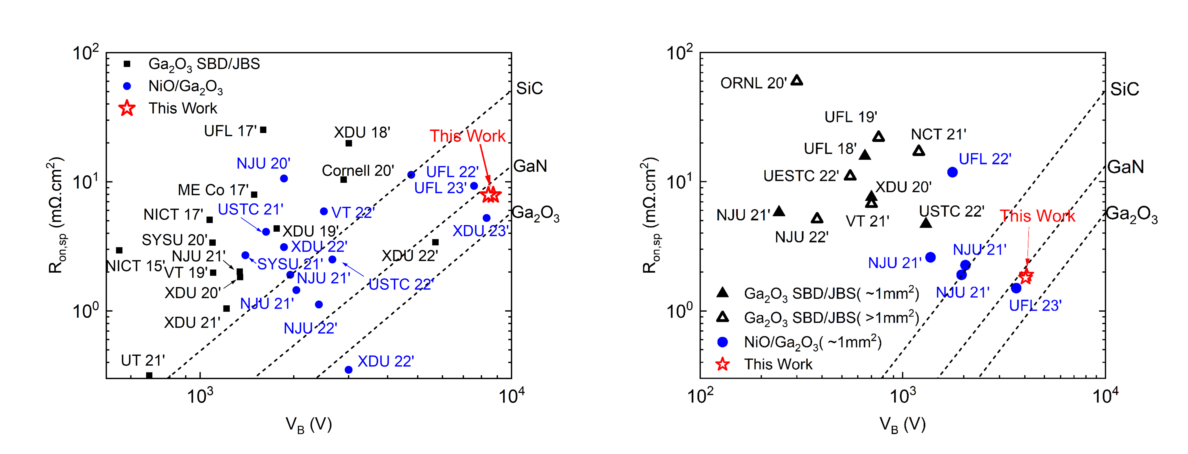
The effect of doping in the drift layer and the thickness and extent of extension beyond the cathode contact of a NiO bilayer in vertical NiO/β-Ga2O3 rectifiers is reported. Decreasing the drift layer doping from 8x10¹⁵ to 6.7x1015 cm-3 produced an increase in reverse breakdown voltage (VB) from 7.7kV to 8.9 kV, the highest reported to date for small diameter devices (100µm). Increasing the bottom NiO layer from 10 to 20 nm did not affect the forward current-voltage characteristics but did reduce reverse leakage current for wider guard rings and also reduced the reverse recovery switching time. The NiO extension beyond the cathode metal to form guard rings had only a slight effect (~5%) in reverse breakdown voltage. The use of NiO to form a pn heterojunction made a huge improvement in VB compared to conventional Schottky rectifiers, where the breakdown voltage was ~1kV. The on-state resistance (RON) was increased from 7.1 mâ¦.cm2 in Schottky rectifiers fabricated on the same wafer to 7.9 mâ¦.cm2 in heterojunctions. The maximum power figure of merit (VB)2/RON was 10.2 GW.cm-2 for the 100µm NiO/Ga2O3 devices. We also fabricated large area (1 mm2) devices on the same wafer, achieving VB of 4 kV and 4.1 A forward current. The figure-of-merit was 9 GW.cm-2 for these devices. These parameters are the highest reported for large area Ga2O3 rectifiers.